

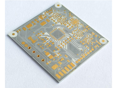
LTCC/HTCC type ceramic substrate
Number of wiring layers: 1-40 layers
Implementation of cavities: blind cavity, stepped cavity, through cavity;
Warping degree: 3.2 ‰ (Max.)
Minimum line width/line spacing: 100 μ m/100 μ m
Minimum aperture/spacing between holes: 100 μ m/150 μ m
By fully utilizing the excellent performance of ceramic materials and the structural characteristics of three-dimensional integration, it is perfectly compatible with various devices (bare chips, packaged devices, heat dissipation components, etc.) and multi chip component assembly processes, which can effectively reduce adverse factors such as signal delay, crosstalk noise, and Ohmic loss generated in interconnection and wiring. It is particularly suitable for high-frequency communication components and high-power modules.